KiCad (and electrical engineering stuff)
Created: 2021-10-16 16:46:41 -0700 Modified: 2022-11-11 17:41:30 -0800
Video series
Section titled “Video series”Starting with this video in the series and taking notes (supplementing with the rest of the Internet where appropriate):
- Printed circuit board (PCB): a board that electrically connects and mechanically supports electrical components. The lines on the board are called “tracks” or “traces” and are typically copper. The copper is laminated onto the substrate: a non-conductive material, typically fiberglass (e.g. FR4 or FR-4 is a composite of fiberglass and epoxy resin; it’s also flame resistant).
- Layers: a single-layer board is the substrate with copper on just one side. A two-layer board would have copper on both sides. More layers can be added, but more substrate has to be added to support this (and they’re typically for more complex PCBs like a Raspberry Pi).
- Solder mask layer: boards are substrate with copper etched or removed so that only the traces and pads you designed are left on the board. However, that copper is susceptible to short circuits. This is where the solder mask layer comes in to protect against the short circuits. It’s usually a lacquer-like polymer (and is typically green) and helps prevent solder from creeping down the traces or jumping between traces.
- Via: an electrical connection between copper layers. It’s essentially a small drilled hole that goes through two or more adjacent layers. The hole is plated with copper that forms an electrical connection through the substrate.
- Pad: an exposed region of metal that the component lead is soldered to.
- Oxidation: copper oxidizes, which can make soldering difficult, so you’ll typically have a surface finish on the copper itself, e.g. electroless nickel immersion gold (ENIG).
- Silkscreen layer: a layer where you can add ink (usually in white) to add text (e.g. to label components), artwork, etc.
- Footprint: the configuration of pads and traces (and holes if it’s through-hole) which mechanically/electrically allow a component to be placed. E.g. Component X may be 3mm across and 5mm tall.
- Reference designator (reference): you may see symbols like “U” for “integrated circuit” or “R” for resistor. See the reference link for the most commonly used designators.
- Layers: a single-layer board is the substrate with copper on just one side. A two-layer board would have copper on both sides. More layers can be added, but more substrate has to be added to support this (and they’re typically for more complex PCBs like a Raspberry Pi).
- Board mounting techniques
- Through-hole mounting (THM): leads on components are inserted through holes in the circuit board. Pro: better withstand mechanical stress. Con: pre-drilling holes is expensive and time-consuming.
- Plated through-hole: if you have a two-layer board (i.e. one with copper on both sides), you can connect the two layers with a plated through-hole, which would have copper electroplated onto the hole itself.
- Surface mounting: components are attached by solder directly onto the surface of the PCB. Pro: both sides of the PCB can be used since there isn’t a hole drilled through it, and surface-mounted devices (SMD) are smaller; both of these result in a greater density of components. Cons: less resistance to mechanical stress, harder to solder by hand.
- Through-hole mounting (THM): leads on components are inserted through holes in the circuit board. Pro: better withstand mechanical stress. Con: pre-drilling holes is expensive and time-consuming.
- KiCad is a collection of programs: they generally let you do the following:
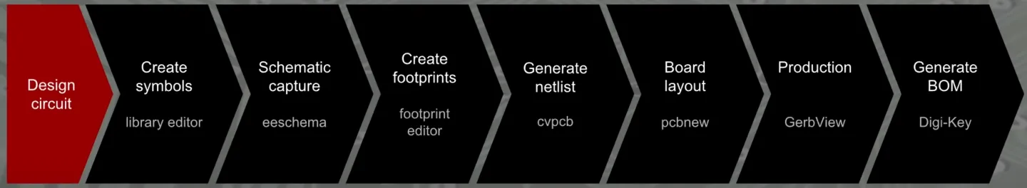
Designing a PCB
Section titled “Designing a PCB”-
Boundaries
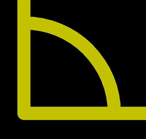
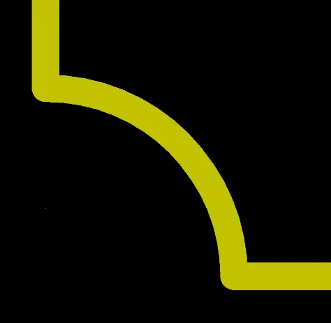
- Edge cuts: these are the boundaries of your PCB. Here’s a great video on how to round corners. Here’s my short summary after struggling for so long:
- First, select your edge-cuts layer by clicking the yellowish square to the left of it so that a black arrow shows next to it:
- Make a right angle using “Add graphic lines”
- Draw an arc going the “wrong” direction (I had to hold ctrl while doing this since one of the lines in the right angle wasn’t aligned to the grid):
- Retract each of the right-angle lines to the curve:
- Right-click the curve, rotate it twice (“R”), then move it to fit (you may also have to drag it from different parts of it to move/snap it; it’s sort of finicky, but it should work)
- First, select your edge-cuts layer by clicking the yellowish square to the left of it so that a black arrow shows next to it:
- Edge cuts: these are the boundaries of your PCB. Here’s a great video on how to round corners. Here’s my short summary after struggling for so long:
-
Routing
-
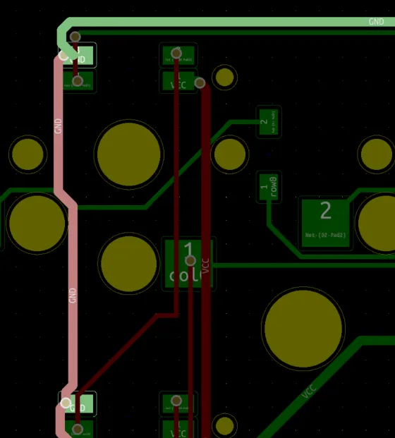
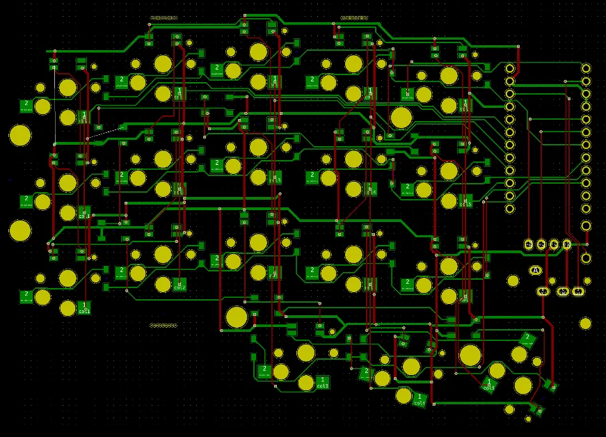
Crossed lines are connections: suppose you have two LEDs connected via a trace and there’s a ground line that you want to route through that connection. If the ground touches the LED trace, then they’re all connected now (which would be bad). Instead, you have to route such that there’s no connection, which means either finding a path around or finding a path through another layer. If it involves another layer, then you’ll need to make two vias and then trace through another layer. For example, in this picture…
-
-
…you can see that no two red lines cross and no two green lines cross. Where this would have happened is at the upper left: there’s a green GND line on top that connects to the upper left pad, so to avoid connecting the bottom left pad to the GND, they put a via on the bottom left pad and another just above the upper left pad, then they switched to the red layer to draw the trace.
-
-


Sending to a manufacturer
Section titled “Sending to a manufacturer”- Free PCBs: check this out—allpcb.com lets you get one totally free PCB per month as long as it meets certain requirements (reference). UPDATE: this was canceled in January, 2022, apparently. 😢
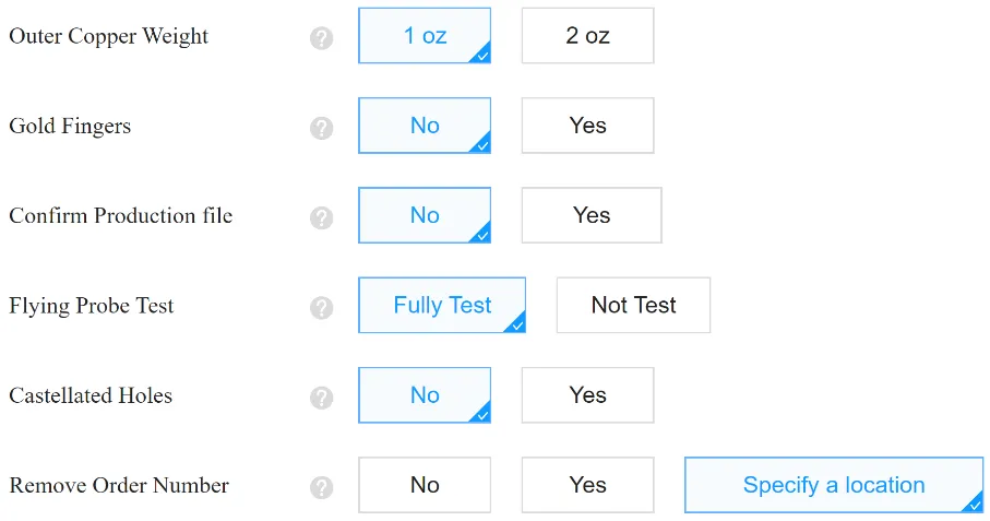
- Generate drill and gerber files (reference): the reference link specifically talks about exporting for JLCPCB.
- On JLCPCB: for my keyboard, I selected:
- Different designs: 2 (because there are 2 PCBs that aren’t connected by traces) (reference)
- Panel by customer
- 1.6mm thickness is apparently the most common (reference)
- LeadFree HASL-RoHS
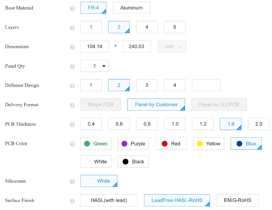
- The merchandise cost 8.40 for 12-20 business days or 2 extra and my other parts should be here in like 19 business days. Total was 6 off, so it was $24.52.
Usage learnings
Section titled “Usage learnings”- Editing the title (the title is the red text at the bottom left): File → Page Settings
- Viewing the back of the PCB: there are two easy options:
- Hide all layers except for something like B.SilkS and then choose View → Flip Board View (at the bottom)
- Enter the 3D viewer (View → 3D Viewer) and then just pan around
- Highlight net: there’s a tool on the right-hand toolbar called “highlight net”. Click it and then an item on the PCB to turn this…
- …into this…
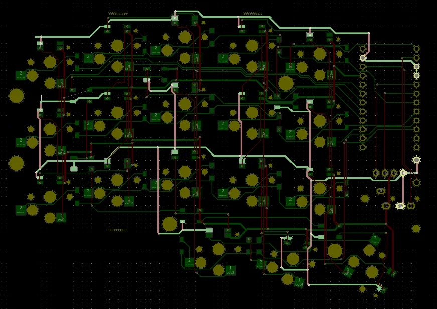
- It makes it easy to see what’s connected.
Ensuring a PCB is good
Section titled “Ensuring a PCB is good”- Design rules check (DRC): in Pcbnew, click the bug icon in the toolbar to run the DRC. It will list any problems or unconnected items.
- Unconnected items: unconnected items are denoted by a white line between two locations (e.g. a track and a via, two tracks, etc.). You can right-click them to select one of those locations whereupon you should see that white line. The fix would be to either delete the items or connect them.
- Avoid ground loops (reference): just read the reference link; it’s easier to see the pictures.
Soldering notes
Section titled “Soldering notes”(writing these mostly for myself based on having made the Corne in late 2021)
- Set up a fan before soldering so that you’re not inhaling fumes.
- Set the soldering iron to 350° C.
- Use a flat cardboard surface in a pinch for soldering so that you don’t ruin the surface you’re working on.
- The diodes I bought say “T4” on them. The triangle on the PCB face toward the “T” side, not the “4” side.
- LEDs are notched. The notch goes toward the corner drawn in the silkscreen on the PCB.
- The LEDs were the hardest to solder. Don’t be shy about trying to cover the whole pad with solder. With the underglow LEDs, make sure to actually make contact between the LED leads and the pads.
- The soldering paste in the kit I got I got is just rosin flux (reference). I found it pretty hard to use (I’d tried with a toothpick). I would probably want a flux pen in the future.
- Taugeshtu: I see lots of people trying to solder with JUST the flux core solder, which is definitely not enough.. Get a no-need-to-wash-off flux, get a syringe, squirt a droplet on the joint; then heat it with iron, then dab solder in. Works wonderfully
- You can use isopropyl alcohol to clean the flux using a toothbrush or Q-tip.
- Reflowing is really helpful if you mess up a joint. It means to heat up the solder that’s already present so that it flows differently this time around. Flux can help with this.
- Sockets (typically Mill-Max, which is just a well-known brand) and pins are so that you don’t have to solder the microcontroller directly to the board. I.e. it will let you solder the microcontroller to the pins, then the pins can connect to the sockets, and the sockets will be soldered to the board.
- The plastic sheaths on the pins are pretty easy to break off if you don’t want them for whatever reason.